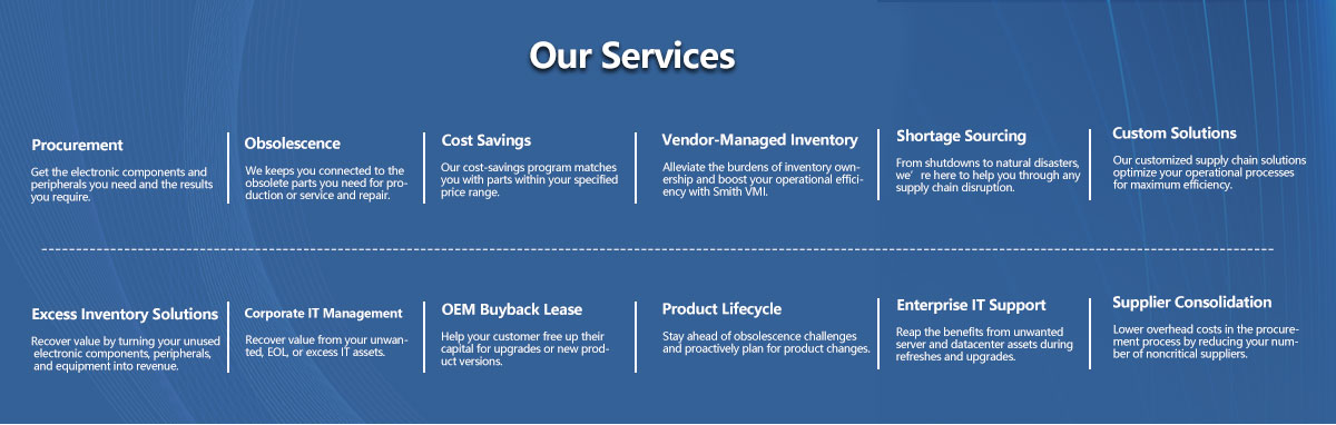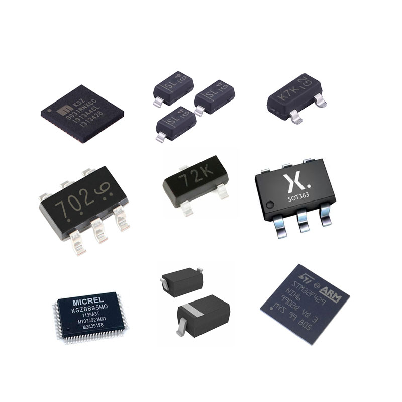
The whole process of chip manufacturing often includes the key steps of wafer production, oxidation, photolithography, etching, thin film deposition, interconnection, testing and packaging. If you want to produce wafers, you need to prepare materials first. In fact, the more commonly used material is silicon. There are many silica sands in nature, but the purity is not enough, so it needs to be refined. When the purity reaches a certain level, it is necessary to remove surface defects through grinding and optical etching processes, and then polish to form a smooth surface, so that a finished wafer with a clean surface can be obtained.
In fact, the role of the oxidation process is to form a protective film on the surface of the wafer, which can effectively protect the wafer from chemical impurities, prevent leakage current from entering the circuit, and prevent the diffusion of the ion implantation process and prevent the wafer from being etched. time slipped. The photolithography step is very important, because the higher the fineness of the circuit pattern, the higher the integration of the finished chip, which is often achieved through advanced photolithography technology.
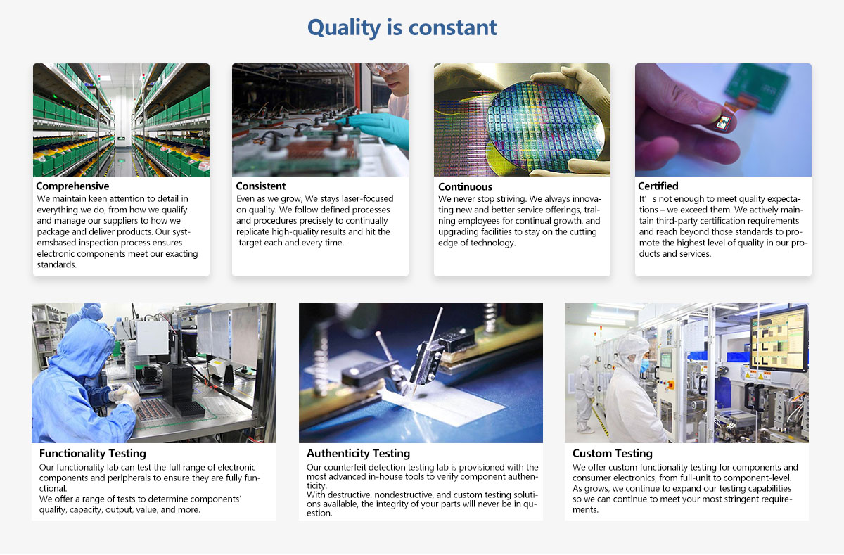
In the process of etching, thin film deposition is required, and each wafer or storage unit is built step by step through the process of thin film deposition. In fact, the purpose of testing semiconductor chips is mainly to check whether the quality of the product reaches a certain standard, so as to eliminate bad products and improve the reliability of the chip.
The above is the whole process of manufacturing chips.